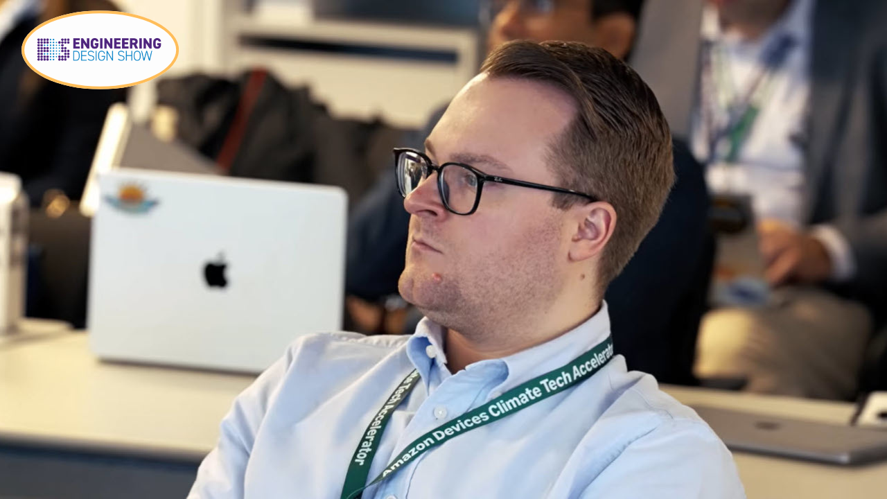
Jiva Materials’ recent experience inside Amazon Devices Climate Tech Accelerator is a clear example of how collaboration between early-stage innovators and established device manufacturers can unlock commercial readiness. For startups working in circularity and low-impact materials, access to structured processes, hard questions and real-world scale can be as valuable as capital.
Sustainable Engineering’s Jon Barrett interviewed Jack on his returned from a two-part program split between San Francisco and Seattle. The goal of the Accelerator was clear but demanding: learn Amazon Devices’ playbook, then apply it to a tangible integration path. The format compressed strategy, writing, lifecycle data and leadership scrutiny into an intense sequence designed to make Jiva’s novel PCB substrate technology legible to a large organisation.
What emerges is a playbook for translating sustainability promises into manufacturing reality. It starts with thinking and writing differently, focuses relentlessly on customer outcomes and ends with quantified impact and a sober look at integration risk. Along the way, the discipline of a global hardware organisation pushes startups to tighten claims, verify numbers and plan for volumes that actually matter.
Jack said: “A key component of the process is called PRFAQ which stands for Press Release and Frequently Asked Questions. Within Amazon it’s about condensing key information into this one document. The takeaway for me was that everything Amazon does is customer driven.”
The PR section forces the technology into a concise, customer-facing narrative, written as if launch were imminent. The FAQ section then drills into 20 set questions that Jiva answered across cost, carbon reduction, scalability and supply chain. For a materials startup, that means pinning down things including lab performance, weight reduction, process changes and end-of-life handling.
Collaboration shaped the commercialisation path
From the outset, Jiva’s engagement was framed around practical integration within Amazon Devices & Services group. Herring explained the devices organisation focuses on hardware and the accelerator was an on-ramp to work through potential commercialization step-by-step. The weeks were structured so learning preceded pitching which itself was anchored in a document everyone had read and annotated.
Jack added that Amazon Devices & Services maintains device life cycle assessments (LCAs) with category breakdowns that align with how Jiva calculates impacts. Having a public reference point made it easier to quantify potential reductions and avoid vague claims. For a startup chasing embodied carbon savings and weight reduction, that kind of granularity is a forcing function for credible modelling.
The ‘future-dated’ press release was particularly revealing. Writing from a point ‘over a year ahead’ sharpened assumptions about evidence needed at launch, pulling customer-relevant attributes to the front. Density reduction, for example, moved from a technical note to a core user benefit, because a lighter device is easier to ship, hold and service.
PRFAQ clarified customer outcomes and technical priorities
The first week in San Francisco was a workshop with a focus on writing discipline. Herring was encouraged to digest the ‘working backwards’ approach and apply it under tight constraints. The result was a sharper, shorter articulation of value that set up the technical deep dive that followed.
Jack said: “I started off with a nine page document. I had to condense that down to three. It was a tough exercise but worthwhile. I’ve never been able to write as concisely as I have now. No weasel words, no long sentences, no unnecessary grammar.”
Jack explained Seattle was the pitching phase: “You meet the decision makers who first read the document in detail and make notes. I was then given the opportunity to introduce myself, followed by questions and answers.”
Written claims are interrogated and discussion digs into assumptions. For a sustainability-led materials business, it means the numbers and manufacturing realities carry the day.
Weight, carbon and energy: quantified drivers of benefit
One of the most practical outputs of the program was a cleaner articulation of Jiva’s value where it matters. For example, density reduction was elevated from a lab metric to a customer and logistics benefit. The interview also underscored the wider systems effect of weight in transport and handling, where small reductions multiply across containers, warehouses and last mile. Framed this way, weight reduction becomes both a user experience win and a distribution efficiency lever.
Jack said: “Our product is 37 per cent lighter than FR4, which translates to a lighter, more enjoyable experience for the end consumer.
“The PRFAQ focused on the environmental impacts our technology offers. The process explored where we are now (68 per cent carbon reduction) and what we could reach when producing at scale (towards 76 per cent carbon reduction). We were also encouraged to look at secondary, downstream benefits such as low temperature soldering which can reduce energy usage and costs by up to 40 per cent.”
End-of-life route was also interrogated. Jiva’s use of natural fibres and solubility enable a different kind of recyclability at teardown and Herring noted that Amazon Devices & Services is encouraging biogenic sequestration in its portfolio. That alignment matters because it links a startup’s material choices to a device maker’s broader sustainability strategy across materials selection, repairability and recovery.
Integration Readiness Level combines technology and manufacturing realities
Engineers involved in innovation likely understand technology and manufacturing readiness levels (TRL/MRL). Amazon Devices & Services takes this further with the Integration Readiness Level (IRL) that aligns technology confidence with manufacturing maturity and supply chain assurance. For a PCB substrate, IRL anchors the conversation in whether a manufacturing line can run at target volumes with available inputs and stable yield.
Jack said: “It’s a way of putting a new technology on a readiness scale for satisfying production volumes.”
IRL also considers raw material availability and overall supply chain factors. In practice, that forces early clarity on sourcing, processing windows and compatibility with downstream assembly. For a circular-economy material, it also invites a broader view of transport and disassembly, which are often where lifecycle benefits show up most clearly.
The headline lesson from Jiva’s accelerator experience is that collaboration works when it produces disciplined thought, tough questions and measurable outcomes. Using this process, if you are responsible for materials selection or product sustainability in an OEM, the path to piloting a new substrate becomes clear.